| The Road to Silicon Valley |
| Written by Historian | |||
Page 1 of 2

The name Silicon Valley is known to people who have never touched a computer. It is the legendary centre of electronics and computing excellence where big companies make large sums of money out of very small things indeed. The strange truth is that the development of Silicon Valley was dependent on a small number of people. The same names occur repeatedly in the companies that came to populate this small region of California and it is as much the people as the place that should interest us. Early Semiconductor DevicesAfter World War II the need to invent something to replace the valve was obvious to everyone but the early science of semiconductor materials was something that developed only slowly. There were already solid state rectifiers - copper oxide rectifiers and the well known “cat’s whisker”, a metal contact attached to a piece of lead sulphide, were in common use. The cat’s whisker was the first metal semiconductor junction device in widespread use and it is sobering to realise that this happened in 1874. The metal rectifier was made from disks of copper oxidised on one side and operated as an effective mains voltage rectifier. Later it was improved by the use of selenium oxide but, despite the fact that these solid state devices were in common use, no-one had much of an idea how they worked.
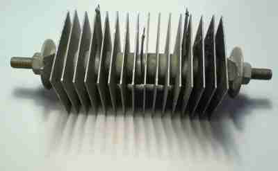
A metal rectifier To understand them it took the development of quantum mechanics and its application to solid state physics. Slowly a theory did develop of how current was carried in non-metallic substances. Physicists such as Nevill Mott in the UK, Boris Davydov in the USSR and Walter Schottky in the US, independently worked out how metal semiconductor junctions function. Early attempts at extending the rectifying mechanism to an amplifier concentrated on using the field effect because it was similar to the way valves operated. However, although the field effect transistor is a very simple concept making one work requires an understanding of the subtle way electrons behave at surfaces. As a result we had to wait many years for the first operational field effect transistor and early solid state electronics was based on the more complex bipolar transistor. The bipolar transistor was invented by John Bardeen, Walter Brattain and William Shockley. The important point is that it would be wrong to believe that it all happened in a logical step-by-step way. Shockley, for example, first proposed a solid state amplifier based on an oxidised copper grid and he and his team concentrated on field effects rather than bipolar junctions. Part of the reason for this emphasis was simply the lack of materials technology.
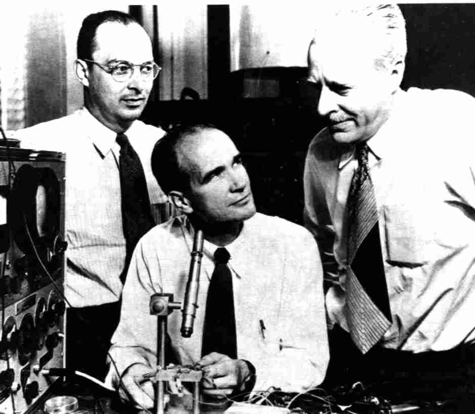
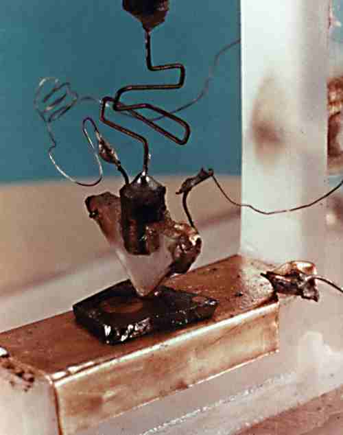
From left to right: John Bardeen, Walter Brattain Two Types of SiliconThe notion that there were two different types of silicon was slow to emerge. At Bell Labs two metallurgists had learned how to purify silicon by pulling a crystal from a molten mass of the material in a vacuum. They obtained relatively pure ingots that behaved in different ways. One type conducted best when biased negatively, another conducted best when biased positively and so they named them n-type and p-type. The problem was that they didn’t know what made the n- and p-type silicon ingots different. They tried the most sensitive chemical analysis techniques available but, whatever the impurities were, they were in such small quantities that they couldn’t be detected. One of the metallurgists thought that he could identify the smell of phosphorus from the oven when the door was first opened - he was right. Eventually they worked out that doping silicon with elements from the same group as phosphorous produced n-type and using elements from the same group as boron produced p-type silicon. The n-type silicon had an excess of electrons available for conduction and p-type had a deficit. This was an elegant and simple discovery and soon they were producing ingots doped to be p-type at one end and n-type at the other. When they sliced the ingot in the middle they had the first p-n junction to experiment with. The Point-Contact TransistorDespite the improvements in materials science, the research group at Bell still concentrated on the field effect theory put forward by Shockley but they had no luck in producing an amplifying device. It is generally assumed that they gave up and moved on to invent the transistor as we know it today, but this isn’t so. They actually succeeded in building a field effect transistor in the week before Christmas 1947 but it would only work immersed in an insulating liquid. A few days later they managed to make the device work, with a drop of water acting as the gate, on a slab of silicon. It worked but it clearly wasn’t a practical device! Four days later they manage to create a workable prototype point contact transistor that was dry. The trick was to place two metal contacts very close together on a bar of silicon. The device was the first transistor but it wasn’t perfect. The need to make two metal contacts so close together made the device unreliable.
The first point contact transistor Shockley believed that it was possible to build a better device - possibly still based on the field effect. Soon after the announcement of the point contact transistor in 1947 Shockley abandoned his search for a field effect transistor and settled on the now familiar pnp sandwich arrangement of the bipolar transistor. He thought it would work but he couldn’t verify his ideas simply because there was no way to build it! It took three more years before the necessary materials science caught up with Shockley’s ideas. Gordon Teal and John Little, working at Bell Labs, had managed to develop methods of pulling doped crystals from a melt. At the time other workers argued that large perfect crystals of silicon were unnecessary and would always be to expensive to work with - but Teal carried on. In 1950 he managed to produce an ingot doped first as p type, then as n type and finally as p type. When this was sliced up the result was a large number of Shockley’s pnp junctions and the era of the modern transistor had started. The junction transistor was more reliable, produced less noise and could handle more power than the point contact transistor. <ASIN:0393318516> <ASIN:0471415413> <ASIN:0762742399> |
|||
| Last Updated ( Thursday, 04 February 2021 ) |