| Raspberry Pi IoT In C - Pi 5 Memory Mapped GPIO |
| Written by Harry Fairhead | ||||||||||||||||||||||||||||||||||||||||||||||||||||||||||||||||||||||
| Wednesday, 10 January 2024 | ||||||||||||||||||||||||||||||||||||||||||||||||||||||||||||||||||||||
Page 3 of 4
Registered IO BlockAt this point you might think that we are ready to access the state of the GPIO lines for general input and output. This isn’t quite the whole story. To accommodate the fact that the processor has two cores, and to make access to important devices faster, there is a special connection between the cores and the GPIO, the RIO or Registered IO Block. Notice that the GPIO lines are multipurpose and to use a GPIO line via the RIO you have to set its mode to RIO via direct access to its control register. The low-order five bits of the GPIO control register set the function of the GPIO line. You can see the values needed for any given function in the documentation, but to assign the GPIO line to RIO control you have to set it to function 0x05. In this sense the RIO is just another peripheral that can take control of a GPIO line. The RIO provides a set of registers that makes using the GPIO much faster and much easier to use. The basic registers are:
Each register holds a bit pattern such that bit n relates to GPIOn. For example, the first bit of OUT sets the level of GPIO 0, the fifth bit of IN reflects the current state of GPIO 5 and so on. There is also a general principle that every register has a set of four aliases. If the register is at address X then:
It is difficult to know from the documentation if there are any exceptions to this, but it does seem to be a general mechanism.
For the RIO registers the availability of XOR, SET and CLR registers is a great simplification. For example, if you want to set GPIO 0 to a high output without modifying any of the other GPIO lines then you would need to first read OUT, OR the value with 0x01 and then store the resulting bit pattern in OUT. Using SET you would simply store 0x01 in SET as the only line to be set is GPIO 0. The RIO registers are at 0x400e0000, which makes its offset 0xe0000. We can use the same technique of defining a struct to allow access to the registers: typedef struct
{
uint32_t Out;
uint32_t OE;
uint32_t In;
uint32_t InSync;
} rioregs;
#define rio ((rioregs *)RIOBase)
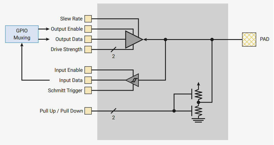
where RIOBase is: uint32_t *RIOBase = PERIBase + 0xe0000 / 4; We can use the same technique to access the XOR, SET and CLR registers: #define rioXOR ((rioregs *)(RIOBase + 0x1000 / 4)) #define rioSET ((rioregs *)(RIOBase + 0x2000 / 4)) #define rioCLR ((rioregs *)(RIOBase + 0x3000 / 4)) PAD ControlUsing the RIO we can read and write the GPIO lines, but there is a further step we have to complete before we can actually make use of them. As described in the previous chapter, each GPIO line has its own PAD and the Pi 5 PAD is very similar to that found in previous devices:
The control of the PAD is also similar to that described in the previous chapter. The PAD registers for the GPIO bank we are using is at 0x400f0000 which means its offset is 0xf0000: uint32_t *PADBase = PERIBase + 0xf0000 / 4; The only complication is that the first register is a VOLTAGE_SELECT register which sets the voltage that all of the GPIO lines in bank 0 work with. A zero sets 3.3V and a 1 sets 1.8V. The default is 3.3V and you can ignore this register unless you need to work at 1.8V. After the VOLTAGE_SELECT register there is a PAD register for each GPIO line:
We can access the PAD registers using: uint32_t *pad = PADBase + 1; For example, if we want to set the PAD to output with a default drive, no pull-up/down, no Schmitt trigger and slow slew rate we would use: pad[pin]= 0x10; Notice that output is set by not enabling input. |
||||||||||||||||||||||||||||||||||||||||||||||||||||||||||||||||||||||
| Last Updated ( Wednesday, 10 January 2024 ) |