| Cache Memory And The Caching Principle |
| Written by Harry Fairhead | ||||
| Thursday, 23 September 2021 | ||||
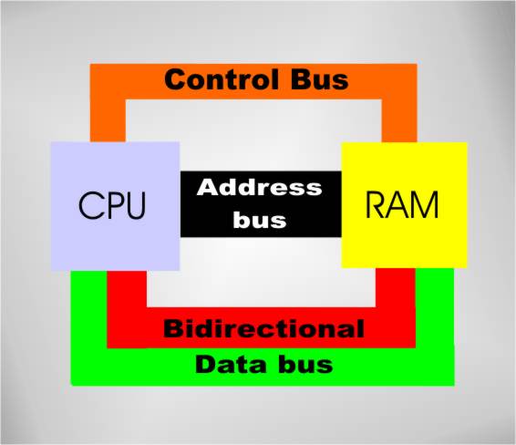
Page 1 of 3 The caching principle is very general but it is best known for its use in speeding up the CPU. We take a look a the basics of cache memory, how it works and what governs how big it needs to be to do its job. Basic memoryBefore getting on with the main topic let's have a quick refresher of how memory systems work - skip to "Waiting for RAM" if you already know about addresses, data and control buses.. Back in the early days of computing things were simple. There was the processor and the memory. The processor stored data in the memory when it wanted to and read the data back when it wanted to. What happens when the processor wants to use memory? Let’s just consider RAM because the only difference between it and ROM is that the processor cannot write data to ROM. The processor has a connection to the memory that allows it to communicate the data being stored or retrieved which consists of a wire for each bit of the address – making an address “bus”. You will also know that the number of memory locations that the processor can address depends on the number of address lines in the bus - each additional address line doubles the amount of memory that can be used. The processor also has a data bus, which it uses to send and retrieve data to and from the RAM. Again the number of wires in the data bus is the number of bits that a single memory location stores and the number of bits transferred in a single memory operation. Notice that only a single data bus is needed as long as it is a “bi-directional” bus. Early microprocessor systems had separate “in” and “out” data buses but the extra complication of all those duplicated wires eventually resulted in the adoption of a bi-directional bus. So far, so good, and in fact nothing much more than was explained about general memory systems in How Memory Works. However, as well as the address and data bus there also has to be a control or system bus. This passes signals to the memory that control exactly what is happening. For example, there is usually a Read/Write (R/W) line, which indicates the direction in which the data bus is operating and whether the memory should read the data on the data bus or use the stored data to set the state of the data bus.
Memory
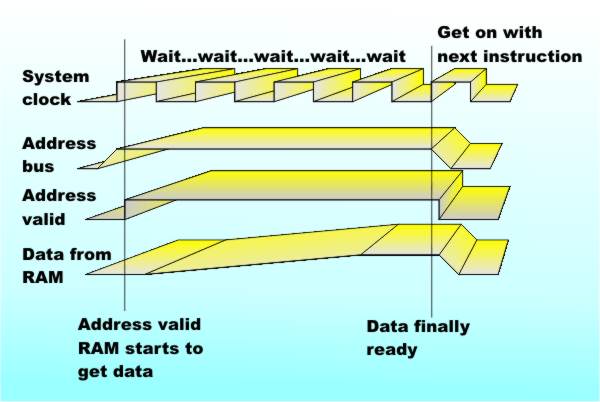
This much is obvious, but there also have to be additional control lines to tell the memory when the address on the address bus is valid – after all you don’t want the memory to respond to the transient addresses that appear on the address bus as it changes from one address to another. There is also usually a control signal that tells the processor that the data on the data bus is valid and so on. The exact arrangement of the control bus varies from processor to processor but you can see what sort of things it has to deal with. Waiting for RAMNow we come to the interesting part – computers are made of components that work at different speeds. One of the control lines usually carries the processor clock because all operations in the machine are linked to this clock. The fastest anything happens within the machine is within one clock pulse. So when the processor wants to write to the memory or read from the memory it takes one clock pulse. Well, no not usually! The problem is that processor chips are made to high cost, high speed, designs. Memory components are usually made to lower cost, slower, designs. Why? Simply because there is only one processor to be bought and paid for but lots and lots of memory chips. What this means in practice is that for quite a long time processors have been able to work much faster than memory. There was a brief period back in the early days when processor chips ran at a clock rate of 1MHz and the memory chips could keep up. As soon as the PC and the second generation processor chips appeared things became more complicated. The memory used, DRAM, needed more than one processor clock pulse time to store and retrieve data and the “wait state” was born. The processor would put the address onto the address bus and the data on the data bus, signal to the memory that it was ready to write data and then it would sit there for one, two, possibly more, clock pulses doing nothing at all until the memory had enough time to store the data. It could then move on to the next instruction.
Waiting for RAM
As you can imagine there was a time when wait states were a big selling point, or rather a non-selling point. The fewer the wait states a machine needed the faster it would run your program but the more money it would cost. Processor clock speeds rocketed from 1MHz, through 4MHz, hit 16MHz and carried on up to today’s maximum of around 4GHz. There is absolutely no way that memory chips could keep up with this sort of amazing speed and be cheap enough to supply the ever increasing amounts of storage needed. There are a number of ingenious intermediate solutions that boost memory thoughput but there is only one really great new idea that solves most of the problems. The solution has in fact been known for some time and was implemented in mainframe and some minicomputer systems. Its working was reasonably well understood but it was fairly complicated and it took time for it to be built into the evolving microcomputer systems. The principle in question was that of using “cache” RAM.

<ASIN:0123229804> <ASIN:0123797519> |
||||
| Last Updated ( Thursday, 23 September 2021 ) |